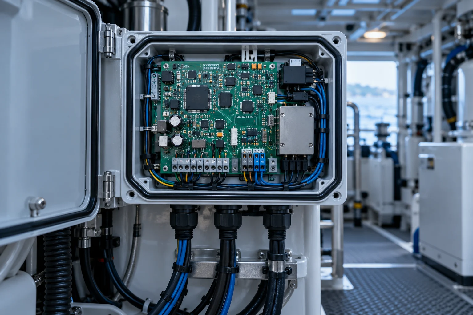
An electronic board that works in the laboratory but resets inside a machine usually cannot be explained by a single “noisy component”. Return-current paths, switching loops, cable connections and the enclosure together determine electromagnetic behaviour. In PCB design, EMC is a layout and current-path problem before it is a list of filters to add at the end.
01Consider current loops before drawing the schematic
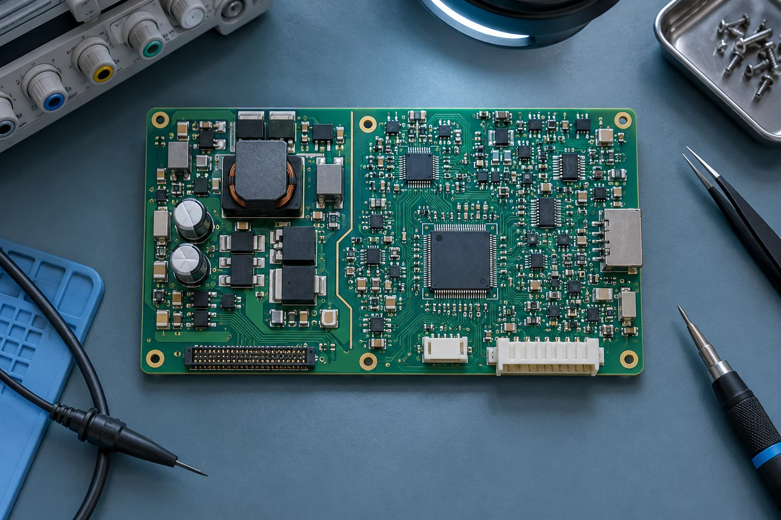
Every signal and supply current has a return path. Loop geometry becomes particularly important for rapidly changing currents. Spreading a switching converter's critical loops over a large area can increase both local voltage spikes and radiated noise. The manufacturer's layout guidance describes physical proximity as well as the order in which components connect.
Plan power, sensitive analogue and communication areas functionally. This does not mean arbitrarily separating each area's ground. Splits that interrupt a signal's return path can force current into a larger loop. Decisions about the ground layer must be made alongside signal routing.
02Decoupling connections matter as much as capacitance
A capacitor placed beside a supply pin may not provide the expected high-frequency performance if connected through long, narrow tracks. Assess loop inductance, connection geometry and access to the return path. Choose capacitor values and packages according to the IC and power distribution network; one universal recipe does not suit every pin.
Keep sensitive references and analogue inputs away from noisy switching nodes. Separation alone is not enough, however: noise coupled through common impedance may also affect measurements. Make it clear where the supply and reference join and which route the return current follows.
03The connector is the board's interface with the outside world
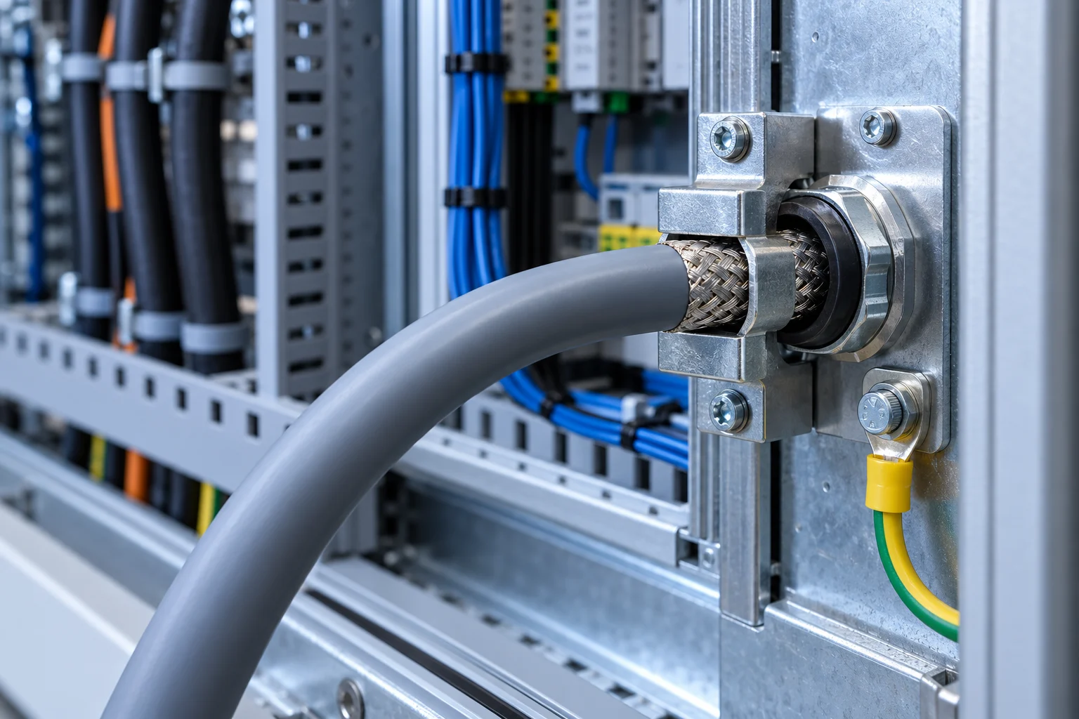
ESD, fast transients and common-mode disturbances arriving through external cables are usually addressed at the entry point. Placing the protective component far from the connector may allow interference to travel into the board. Directing transient current to the correct destination is as important as selecting the right protective component.
| Area | Physical point to inspect |
|---|---|
| Switch-mode power supply | High-di/dt loop and feedback path |
| Analogue input | Reference, common impedance and input filtering |
| Communication | Trace geometry, termination and protection return path |
| Connector | Chassis connection and transient-current path |
| Clock / processor | Edge rates, nearby return paths and supply stability |
04Select the analogue filter for the measurement requirements
An input filter can help with a slowly changing sensor value, but its delay must suit the control requirements. For example, a simple RC circuit with R = 1 kΩ and C = 100 nF has a time constant of 100 µs and an approximate cutoff frequency of 1.59 kHz. This is only an ideal first-order filter calculation.
The ADC input structure, source impedance, sampling time and protection components affect the actual result. Use calculation, simulation and measurement together. Increasing software averaging to remove noise must not conceal a disconnected sensor or a sudden process change.
05Do not let the measurement setup introduce errors
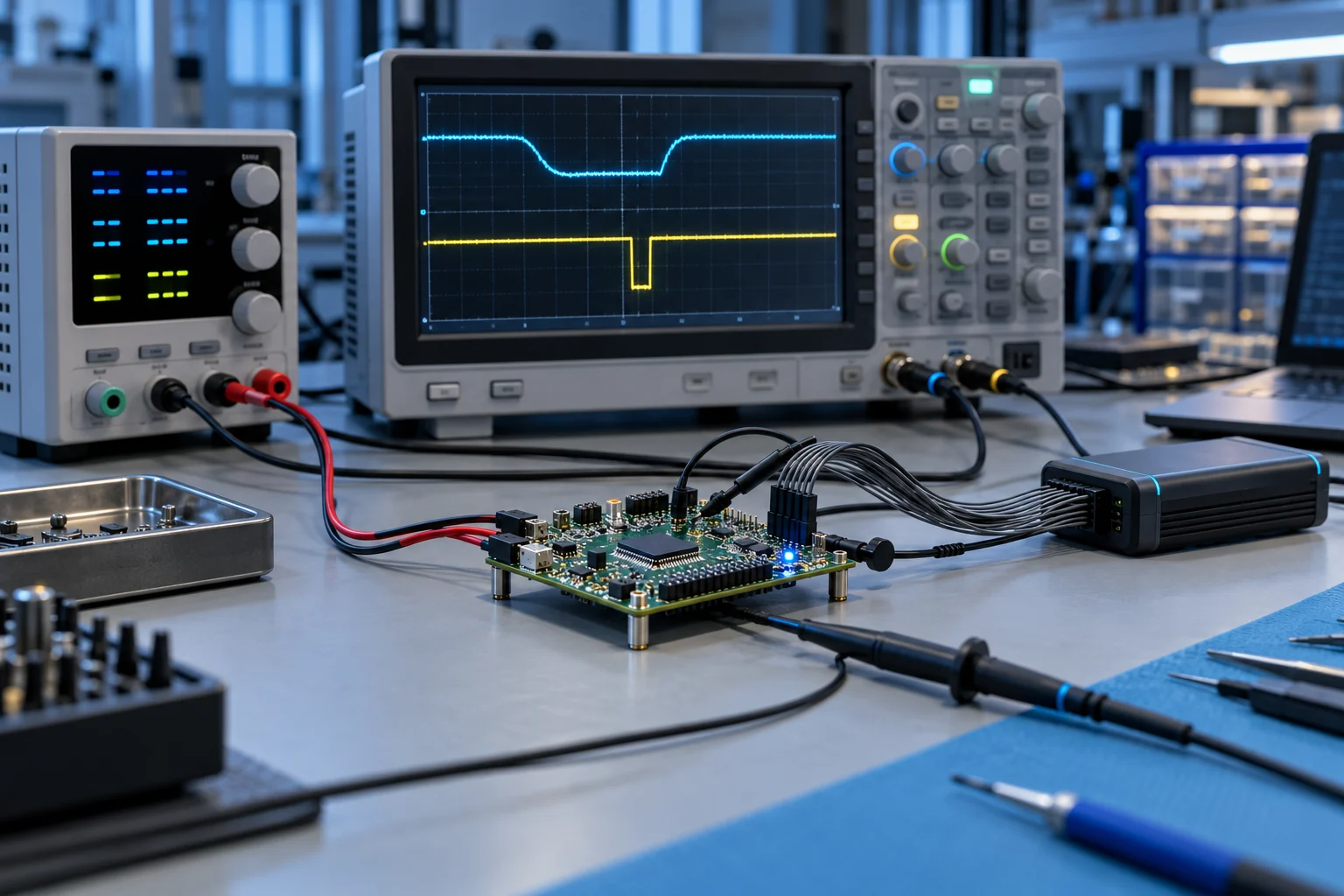
A long oscilloscope ground lead can add ringing to the measured waveform. Check how the probe connection and measurement bandwidth affect the result. Switching nodes and high common-mode voltages particularly require suitable measurement methods. Testing energised high-voltage areas requires competent personnel and appropriate equipment.
When investigating a reset problem, examine the reset line and event-synchronous transients, not merely the processor supply's average value. An event occurring when a motor starts requires different test conditions from continuous measurement noise. Changing one variable per test makes it easier to identify which measure works.
06Make prototype verification part of the design
Include conditions such as cable length, load, supply limits and temperature in the test plan. Perform pre-compliance tests as close as possible to the final product and cable arrangement. A clean result from the board alone does not prove that the complete device meets EMC requirements.
The final revision should record not just “filter added” but the measured symptom, the layout changes and the retest results. The aim is to move from a prototype that happens to work to a design that can be reproduced in a controlled way.
07Example verification scenario
Suppose an analogue input exhibits a brief spike when a load switches. Record raw ADC data, the analogue reference and the supply synchronously with the event. Then assess the critical return path or input filter by making one change at a time. Making the symptom disappear through increased averaging of the displayed number does not prove that the board's underlying behaviour has improved. At acceptance, also check measurement delay and response to actual process changes to demonstrate that noise reduction has not impaired the function.
Technical references and further reading
For product- and version-specific values, the relevant manufacturer's current documentation should be taken as the reference. The calculations and scenarios above are engineering examples for illustrative purposes.